Questions in Electronics are simple at the Higher Secondary/Plus two level. Many of you might be interested in Electronics and your attitude towards this subject will make it seem to be simpler!
Consider the following MCQ which appeared in AIEEE 2003 question paper:
The difference in the variation of resistance with temperature in a metal and a semiconductor arises essentially due to the difference in the
(a) variation in the scattering mechanism with temperature (b) crystal structure (c) variation in the number of charge carriers with temperature (d) type of bonding
The correct option is (c). On raising the temperature of a semiconductor, more charge carriers are produced by the breaking of the covalent bonds, unlike in the case of a metal. Therefore, as you might have noted, semiconductors have negative temperature coefficient of resistance.
Now, consider the following question:
In an npn power transistor, the collector current is 20 mA. If 98% of the electrons injected in to the base region reach the collector, the base current in mA is nearly
(a) 2 mA (b) 1 mA (c) 0.5 mA (d) 0.4 mA (e) 0.2 mA
Since 98% of the electrons reach the collector, the collector current is 98% of the emitter current and the base current is 2% of the emitter current. As the collector current is nearly equal to the emitter current, the base current is 2% of the collector current. Therefore, base current = 20×2/100 = 0.4 mA [Option (d)].
The following question involving the common base current transfer ratio (current gain) α also is simple:
The current gain α of a transistor is 0.995. If the change in emitter current is 10 mA, the change in base current is
(a) 50 μA (b) 100 μA (c) 500 μA (d) 25 μA (e) 5 μA
We have ∆IB = ∆IE-∆IC where ∆IB, ∆IE and ∆IC represent the changes in the base current, emitter current and the collector current respectively.
Since α = ∆IC/∆IE, we have, ∆IC = α∆IE = 0.995 ×10 = 9.95 mA.
Therefore, change in base current, ∆IB = 10 – 9.95 = 0.05 mA = 50 μA
The following question is designed to check whether you have grasped the method of transistor biasing in the simplest possible practical circuit:
Therefore, change in base current, ∆IB = 10 – 9.95 = 0.05 mA = 50 μA
The following question is designed to check whether you have grasped the method of transistor biasing in the simplest possible practical circuit:
In the common emitter amplifier circuit shown, the transistor has a current gain β equal to 400. The collector load resistor RL = RC =3kΩ. If the collector-to-emitter voltage under no-signal (quiescent) condition is to be equal to half of the supply voltage VCC, what should be the value of the base biasing resistor RB? (Neglect the base to emitter voltage drop)
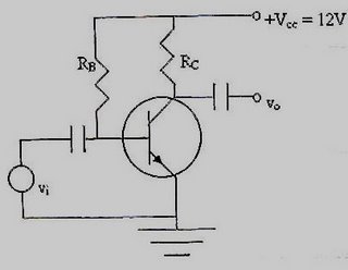 (a) 2.4 MΩ (b) 1.2 MΩ (c) 120 kΩ (d) 6 MΩ (e) 600 kΩ
In the circuit, the supply voltage used is 12 volts and half of it (6V) should appear between the collector and emitter. The remaining half (6V) should appear across the 3 kΩ collector load resistor, on account of the collector current flowing through it.
Therefore, collector current, IC = 6V/3kΩ = 2 mA. [Note that we have substituted the resistance in kilo ohm itself to obtain the collector current in milliampere].
We have IB = IC/β = 2 mA/400 = 0.005 mA = 5 μA.
Therefore, 5 μA should flow through the base biasing resistor RB. Since the base to emitter voltage drop is allowed to be neglected in the question, the voltage across RB is the full supply voltage, 12V. [If you cannot neglect the base to emitter voltage, you will have 11.3 volts instead, in the case of a silicon transistor, since you will have to subtract the forward voltage of 0.7 volts].Therefore, RB = 12V/5μA = 2.4 MΩ [Option (a)].
[Note that we substituted the current in microampere itself to obtain the resistance in megohm (mega ohm).
Now, what is the function of the capacitors on the input side and the output side of the amplifier circuit shown above?
Note that they are meant for preventing the direct biasing voltages from reaching the signal source and the load and for allowing the varying signal voltages to pass through.
Let us consider another question:
In a common emitter amplifier circuit drawing a quiescent collector current of 1 mA, the input resistance of the transistor is 1.2 kΩ and the collector load resistance is 3 kΩ. If the common emitter current gain of the transistor is 400, what is the voltage gain of the amplifier?
(a) 500 (b) 600 (c) 700 (d) 800 (e) 1000
The quiescent collector current of 1 mA given in this question is just a distraction.
The voltage gain (or, voltage amplification, Av) of a common emitter amplifier is given by Av = βRL/Ri where RL is the load resistance and Ri is the input resistance of the amplifier. Therefore, voltage gain = 400×3/1.2 = 1000. [Note that we have substituted the resistance value in kilohm (kilo ohm) itself since we have a ratio of resistances in the expression].
Consider now the following three questions which appeared in Kerala Engineering Entrance 2006 test paper:
(1) If α and β are the current gains in the CB and CE configurations respectively of the transistor circuit, then (β – α)/αβ =
(a) ∞ (b) 1 (c) 2 (d) 0.5 (e) zero
We have, β = α/(1- α). Therefore, the given ratio, (β – α)/αβ = [α/(1- α) – α]/αβ = [1/(1- α) -1]/β = [1-(1- α)]/(1-α)β = α/(1- α)β = β/β =1. Therefore, the correct option is (b).
(2) The number densities of electrons and holes in pure germanium at room temperature are equal and its value is 3×10¹⁶ per m3. On doping with aluminium the hole density increases to 4.5×10²² per m3. Then the electron density in doped germanium is
(a) 2×10¹⁰m-3 (b) 5×10⁹m-3 (c) 4.5×10⁹m-3 (d) 3×10⁹m-3 (e) 4×10¹⁰m-3
(a) 2×10¹⁰m-3 (b) 5×10⁹m-3 (c) 4.5×10⁹m-3 (d) 3×10⁹m-3 (e) 4×10¹⁰m-3
This is a very simple question based on the law of mass action, NeNh = Ni2 , where Ne and Nh are the number densities (number per unit volume) of the electrons and holes respectively in the doped semiconductor and Ni is the number density of electrons as well as holes in the intrinsic (pure) semiconductor.
Therefore, Ne = Ni2/Nh = (9×1032)/(4.5×1022) = 2×10¹⁰ m-3.
(3) The input resistance of a CE amplifier is 333 Ω and the load resistance is 5 kΩ. A change of base current by 15 μA results in the change of collector current by 1 mA. The voltage gain of the amplifier is
(a) 550 (b) 51 (c) 101 (d) 501 (e) 1001
The current gain of the transistor used, in the common emitter configuration is β = ∆IC/∆IB = (1000 μA)/(15 μA) = 1000/15. [Note that we have converted the collector current into micro ampere since the base current is in micro ampere].
The voltage gain of the amplifier is βRL /Ri = (1000/15) ×(5000/333) = 1001.
Here is a question which appeared in IIT 1998 entrance test paper:
In a p-n junction diode not connected to any circuit,
(a) the potential is the same everywhere
(b) the p-type side is at higher potential than the n-type side
(c) there is an electric field at the junction directed from the n-type side to the p-type side
(d) there is an electric field at the junction directed from the p-type side to the n-type side.
Even if no voltages are applied to a junction diode, the n-side is at a higher potential (of a few hundred millivolts, the exact value depending on the type of the semiconductor) compared to the p-side. This results due to the diffusion of electrons from the n-side to the p-side and similarly, the diffusion of holes from the p-side to the n-side. The n-side is therefore left with a net positive charge and the p-side is left with a net negative charge. This inherent reverse bias across the junction therefore produces an inherent electric field at the junction, directed from the n-type side to the p-type side[Option (c)].
No comments:
Post a Comment